

Half-Bridge Driver ICs & Power Stages: Topology, LLC, Design & Troubleshooting

Global electronic component supplier ERSAELECTRONICS: Rich inventory for one-stop shopping. Inquire easily, and receive fast, customized solutions and quotes.
1) What is a Half-Bridge? (Definition & Role)
Answer: Two switches in series across a DC bus; the midpoint drives the load; requires dead-time; no polarity reversal.

How it works (Midpoint node & average effect)
The high-side (HS) and low-side (LS) switches commutate the midpoint node Vmid between 0 and Vbus. With a filter or load averaging, the DC output approximates Vout ≈ D · Vbus, where D is HS on-time duty cycle. Example: with Vbus=24 V and D=0.40, Vout≈9.6 V. Current freewheels through body diodes when the complementary device is off.
Why use a half-bridge?
- Fewer devices and simpler drive than a full-bridge.
- Excellent for SMPS primary stages and each phase of motor drives.
- Good efficiency with proper dead-time and gate return layout.
What it doesn’t do
- No intrinsic polarity reversal (unlike a full-bridge).
- Requires dead-time to prevent shoot-through.
- Not a rectifier; not a Wheatstone “half-bridge” strain-gauge connection.
Engineering essentials (safety & reliability)
- Dead-time ≥ device turn-off time + Miller plateau margin, to avoid HS/LS overlap.
- Plan diode/freewheel paths and keep the gate return loop tight (Kelvin source when possible).
- Common bring-up risks: insufficient dead-time, boot capacitor undervalued, poor probe grounding.
Key relation: Vout ≈ D · Vbus, with D set by high-side on-time (after dead-time enforcement).
Next: Half-Bridge vs Full-Bridge, LLC & ZVS basics, Gate-Driver IC Selection.
Designing for 12–48 V small/medium power? Jump to Driver IC Selection or Submit your BOM (48h) for a discrete vs integrated half-bridge plan.
2) Half-Bridge vs Full-Bridge / Push-Pull / HVDC (Which to choose)
Quick answer: Need polarity reversal at the load? Choose an H-bridge (motors) or a full-bridge (isolated DC-DC). Need a simpler stage without polarity reversal? A half-bridge fits well for SMPS primaries and motor phases. Push-pull is cost-lean for low–mid power but demands strict transformer reset symmetry. HVDC is grid-scale—out of board-level scope.
| Topology | Device Count (power switches) |
Polarity Capability | Voltage Utilization* | Transformer Reset | EMI Tendencies | Control / Driver Complexity | Typical Power Range | Typical Applications |
|---|---|---|---|---|---|---|---|---|
| Half-Bridge (SMPS / power stage) | 2 | No (midpoint only) | ≈½·Vbus at primary/load | Natural (balanced) | Moderate dv/dt; fewer transitions | Low–Med (dead-time; HS bootstrap/isolated) | ~50–800 W (isolated SMPS typical) | SMPS primary, motor phase, class-D stages |
| Full-Bridge (PSFB / phase-shift) | 4 | Yes (effective bipolar drive) | ≈1·Vbus (≈2× half-bridge) | Natural (bipolar excitation) | Higher edges; often mitigated by ZVS | Med–High (phase-shift, sync rect, timing) | ~500 W–kW+ | High-power isolated DC-DC, inverters |
| H-Bridge (motor) | 4 | Yes (direct load reversal) | ±Vbus across load (no transformer) | N/A (no transformer) | CM noise via long motor leads; edge shaping helps | Med (PWM, dead-time, current sense, brake) | Tens of W → kW (by motor) | DC/BLDC/Stepper drives |
| Push-Pull (isolated) | 2 (primary) | Bipolar primary via transformer (output rectified) | ~full-bridge-like (ideal case) | Sensitive to imbalance; needs proper reset | Moderate; spikes if reset poor | Low–Med (duty control; reset management) | ~20–400 W (freq & magnetics dependent) | Cost-lean isolated DC-DC |
| HVDC (grid-scale) | Many (valves/modules) | Four-quadrant / polarity reversal (system-level) | Grid-level | System-level | Grid compliance focus | Very high | MW–GW | Transmission (not board-level) |
* Voltage utilization is indicative; practical values depend on timing, parasitics, and modulation (e.g., ZVS in PSFB).

- Polarity reversal? Yes → H-bridge (motor) or Full-bridge (isolated DC-DC). No → go on.
- Isolation & power tier? kW-class or higher efficiency → Full-bridge (PSFB); mid-power (≤~800 W) → Half-bridge; cost-lean low–mid → Push-pull (mind reset).
- EMI & control budget? Limited resources → Half-bridge/Push-pull; advanced control allowed → Full-bridge with ZVS.
- Parts & cost balance: Switch count, driver channels, magnetics volume, heat. Pick the best trade-off.
Note on HVDC: “Half/Full-bridge” in HVDC refers to converter valves/modules within LCC/VSC systems, enabling four-quadrant power flow and polarity reversal at grid scale. It is a different layer from board-level SMPS or motor bridges covered here.
Next: LLC & ZVS basics, Gate-Driver IC Selection.
DC-motor or isolated DC-DC, but not sure which topology to pick? Submit your BOM (48h) and get a three-metric trade-off: duty-cycle range, efficiency, and BOM cost.
3) Devices & Building Blocks (MOSFETs, Gate Network, Modules)
Core stack (from switches to protection)
- Power devices: MOSFET / IGBT / SiC / GaN (select by voltage & switching frequency).
- Gate driver: high/low-side driver (bootstrap vs isolated), UVLO, CMTI, Miller clamp capability.
- Gate network: split
Rg,on/Rg,off, clamp/TVS, RC/RCD snubber; Kelvin source return. - Supply & sensing: bootstrap capacitor, shunt/Hall sensing, DESAT or fast OCP.
- DC-link & loops: electrolytic + film + local MLCC; keep HS loop & gate loop minimal.

Device parameter priority (what to weigh first)
| Parameter | Why it matters | Rule of thumb / Target | Notes & pitfalls |
|---|---|---|---|
| Voltage rating & derating (VDS) | Survive bus + overshoot; headroom for ringing. | ≥1.25× Vbus for low-V; up to 1.4× at high-V or poor layout. | Validate with worst-case transient & temperature. |
| Gate charge (Qg) | Sets drive current need & switching loss. | Lower Qg for high-fsw; size driver to deliver peak source/sink. | Beware Qg vs RDS(on) trade (FOM). |
| Miller charge (Qgd) / Crss | Controls Miller plateau; susceptibility to false turn-on. | Prefer low Qgd/Crss; use split Rg & Miller clamp. | High dv/dt + high Crss ⇒ shoot-through risk. |
| Output capacitance Coss / Energy Eoss | Dominates turn-on loss & ringing at high V. | Minimize Coss/Eoss for efficiency at high-V, high-fsw. | Check Coss(V) curves; not constant. |
| Reverse recovery (Qrr, trr) | Freewheel losses & spikes in hard commutation. | Choose soft/low Qrr; SiC/GaN ≈ near-zero Qrr. | Body diode may need external Schottky at low-V. |
| dv/dt & di/dt capability | EMI, false turn-on, device stress. | Match with driver CMTI; shape with Rg(on/off) & snubber. | Test on hardware; datasheet limits are idealized. |
| Thermals (RθJC/RθJA, Tj,max) | Sets power density & reliability margin. | Design for ΔT with worst-case loss; ensure heatsinking path. | High-density packages demand good copper & TIM. |
| Package inductance (Lpkg) / Kelvin source | Limits edge speed; causes overshoot & ringing. | Prefer LFPAK/QFN/DirectFET-like; use Kelvin source pins. | Route the gate return directly to source-sense. |
Modules vs discretes (which path fits your constraints)
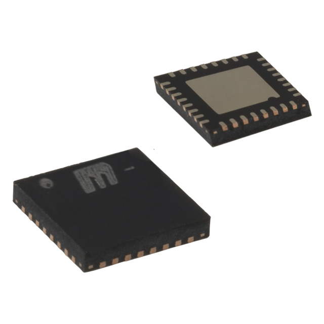
Integrated power stages / modules (GaN, DrMOS, power stage)
- Minimal loop inside package ⇒ higher fsw & efficiency, compact layout.
- Driver & switches pre-matched; faster bring-up.
- Trade-offs:
- High heat density; limited tweakability; voltage window & availability constraints.
- Example: TI LMG5200 (GaN half-bridge), PC VRM-class DrMOS for low-V bucks.
Discrete path (driver IC + MOSFET/IGBT/SiC/GaN)
- Thermal & package freedom; easier cross-brand pin-compatible swaps.
- Scales to ≥600 V/kW; custom protection & sensing.
- Trade-offs:
- Layout/parasitics management required; more parts & validation effort.
Voltage bands quick guide:
- 30–100 V: high current buck/motor phases → low Qg, low Coss MOSFETs or DrMOS/power-stage; prioritize driver peak current.
- 100–650 V: isolated SMPS/inverters → SJ MOSFET or GaN; watch Eoss and turn-on loss.
- ≥650–1200 V: PFC/inverters → SiC MOSFET or IGBT + isolated driver; emphasize CMTI, gate clamp, DESAT.
Is a MOSFET a transistor?
Yes. A MOSFET (Metal-Oxide-Semiconductor Field-Effect Transistor) is a type of transistor. In half-bridges it acts as a high-speed switch driven by a dedicated gate-driver IC.
Discrete path: try TI UCC27211A / LM5106, ST L6398, Renesas HIP2101, onsemi NCP51561, Microchip MIC4605(Melexis partial system-level motor drive);pair with MOSFETs by your 30–100 V or 100–650 V band.
Integrated path: GaN/power stages (e.g., TI LMG5200, DrMOS classes) for high-fsw, compact layouts.
Send Vbus, power, fsw, ambient, Qg and we’ll return two parallel designs (discrete vs integrated) with thermal notes and availability within 48 hours. Submit your BOM (48h)
Next: Gate-Driver IC Selection, Design Calculations & Bring-Up.
4) SMPS / Inverter / LLC (Power Applications)
Quick take: Half-bridge is a workhorse for isolated DC-DC and inverter stages. In LLC half-bridge, the resonant tank (Lr/Cr/Lm) enables ZVS for primary switches over a wide load range. Watch the light-load trap: poor Lm/k selection or timing can drop ZVS. When power climbs to kW-class or you need wider gain, consider PSFB (full-bridge, phase-shift).
Where half-bridge fits in SMPS & inverters
- Isolated DC-DC (SMPS): PFC bus 380–420 V → 12/24/48 V. Mid-power designs often use half-bridge + LLC.
- Inverters: DC→AC stages (UPS/PV/motor). Half-bridge and full-bridge both apply; choice depends on voltage utilization & polarity needs.

LLC primer (tank, regions, and why ZVS happens)
- Tank: series
Lr+Crwith a magnetizing shuntLm. Definek = Lm/Lr(typ. 3–7). - Normalized frequency:
fn = f / fr, wherefr = 1/(2π√(Lr·Cr)). - Operating regions: inductive (f > fr) → easy ZVS for primary; capacitive (f < fr) → avoid sustained operation.
- Load factor: quality factor
Q = R'ac / (ωr·Lr)(withR'acreferred to primary) shapes the gain curve and frequency excursion.
ZVS condition (rule-of-thumb): iLm,turn-on ≳ icoss + iload,reflected, where icoss ≈ ΔQoss / tdead. At light load/high Vin, reflected load current is small; ZVS relies on Lm. Too small Lm (low k), insufficient dead-time, or high Eoss parts can drop ZVS.
LLC half-bridge design flow (10 steps)
- Specs: Vin range, Vout, Pout, η target, thermal/volume, EMI/regulatory.
- Turns ratio N: derive from extreme Vin/Vout and rectification method (diode vs SR).
- Select fr & window: e.g., 0.6–1.6× fr. Higher f → smaller magnetics, higher switching loss (GaN helps).
- Pick k = Lm/Lr: 3–7 typical. Larger
kaids light-load ZVS but raises circulating energy. - Choose Q @ rated: ~0.4–0.8 to balance gain slope vs frequency excursion.
- Solve Lr/Cr:
fr = 1/(2π√(Lr·Cr)),Zr = √(Lr/Cr). Use Q and R'ac to back-solve Lr, Cr. - Set Lm:
Lm = k·Lr. Recheck ZVS margin across Vin/load (use ΔQoss vs tdead estimate). - Choose switches: SJ MOSFET / GaN / SiC per Vbus & fsw; prioritize low
Eoss, lowQgd, adequate dv/dt. - Rectification: diodes vs SR (timing & reverse conduction management).
- Thermal & EMI checks: core/copper loss, skin effect, leakage & snubbers, CM paths & Y-caps.
Key formulas:
- Resonance:
fr = 1/(2π√(Lr·Cr)), characteristic impedance:Zr = √(Lr/Cr). - Soft-switching (approx.):
iLm,turn-on > icoss + iload,reflected, withicoss ≈ ΔQoss/tdead. - Primary current (near resonance, quick screen):
Ipk,pri ≈ Vbus / Zr. - Flux density (sine approx.):
Bpk ≈ Vpri,rms /(4.44·N·Ae·f).
Stay with LLC half-bridge when…
- 200–800 W mid-power, compact board, low acoustic/EMI needs.
- Reasonable light-load efficiency; GaN available for higher fsw.
- Moderate gain range suffices (Vin variation limited).
Switch to PSFB (full-bridge) when…
- ≥1 kW, wide Vin or long hold-up, need broader gain window.
- Consistent ZVS over wider load; heavy SR currents on secondary.
- Accept higher control/driver complexity & circulating energy.
Common pitfalls (save a week on bring-up)
- Mistaking leakage for
Lr→ actualfrshifts; measure & de-embed parasitics. Crbias/temperature drift → frequency drift; pick C0G/NP0 or derate X7R with margin.- Dead-time vs SR timing conflict → cross-conduction; validate with scope at min/max Vin.
- Magnetics: overly aggressive
Bmax, excessive fill factor, poor layer stacking → higher losses/leakage. - EMC: HS node couples to primary; plan CM path, shielding layers, and Y-cap placement early.
See also: Gate-Driver IC Selection, Design Calculations & Bring-Up, PCB Layout & EMI.
Building a 400→12 V or 54→12 V LLC? Send fsw, Pout, thermal space, and Vin/Vout to get a 48-hour three-link pack: Driver IC + MOSFET/GaN picks + initial tank sizing with ZVS coverage check. Submit your BOM (48h)
5) Motor Control (Half-Bridge in BLDC/DC Drives)
In motors, each phase is driven by a half-bridge (three phases ⇒ six switches). A full H-bridge (two half-bridges) is used for brushed DC to reverse polarity. Voltage classes: 12–60 V robots/AGV/auto-LV, 100–200 V tools/UAV, 300–650 V appliances/industrial mains.

PWM & dead-time
- Modulation: edge-aligned vs center-aligned; center-aligned generally lowers torque ripple/EMI for BLDC/FOC.
- Dead-time: must exceed device turn-off + Miller plateau margin. Apply dead-time compensation in FOC/SVPWM to correct vector error.
- Synchronous freewheel: replacing body-diode with FET cuts loss but increases overlap risk—validate dead-time across temp/lot spread.
Current sensing without saturation
- Sense location: low-side shunt (cheap, small CM); phase shunt (best dynamic info, harsher common-mode); bus shunt (simple, needs reconstruction).
- Front-end: low-TC shunt + CSA/isolated amp with high CMRR and PWM-recovery; verify input CM range over PWM duty.
- Sampling window: avoid PWM edges; add blanking; match op-amp/CSA recovery to your PWM frequency.
- Layout: Kelvin-sense the shunt; short return to amp; small RC to tame spikes.
Protection & robustness
- Over-current: low-side/phase shunt + fast comparator; high-voltage SiC/IGBT stages use DESAT with soft turn-off.
- UVLO & interlock: prevent half-on states; ensure gate rails are valid before PWM enable.
- dv/dt & CMTI: long leads elevate CM noise—spec high-CMTI drivers and tune
Rg,on/off. - Over-voltage (regen): regenerative braking raises DC-bus; use brake chopper/dump resistor or active clamp; supervise bus voltage.
- EMI mitigation: output RC snubbers, CM chokes, shielded cable with proper bonding.
Quick-pick gate-driver ICs (by voltage & protection needs)
| Device | Voltage Band | Isolation / Bootstrap | Drive Strength (src/sink) | CMTI / dv/dt Robustness | UVLO (HS/LS) | Miller Clamp | Protections | Notes / Fits |
|---|---|---|---|---|---|---|---|---|
| TI UCC27712 | Up to ~600 V bus | HV bootstrap (HS/LS) | High (peak A class) | High-CMTI driver family | Yes / Yes | Varies by option | Shoot-through prevention features | BLDC mains-derived drives; offline PFC/INV stages |
| ST L6398 | Up to ~600 V bus | HV bootstrap (HS/LS) | Med-High | Robust dv/dt tolerance | Yes / Yes | — | OC handling support via externals | Appliances, HVAC inverters |
| Renesas HIP2103 | ≤100 V bus (LV) | Bootstrap (LV half-bridge) | Med (A-class) | Good dv/dt tolerance (LV) | Yes / Yes | — | Shoot-through prevention logic | 12–60 V BLDC/servo phases |
| onsemi FAN7392 | Up to ~600 V bus | HV bootstrap (HS/LS) | Med-High | High dv/dt tolerance tier | Yes / Yes | — | Logic interlock options | Fans, pumps, white goods |
| Microchip MIC4605 | ≤85–100 V bus (LV) | Bootstrap (LV half-bridge) | Up to ~4 A pk class (family) | Good (LV) | Yes / Yes | Adaptive dead-time (family) | Shoot-through prevention; OC via externals | 12–48 V BLDC/BDC, drones/tools |
| NXP GD3160 | 600–1200 V SiC/IGBT | Galvanic isolation + DESAT | High (configurable) | Very high CMTI (SiC-class) | Yes / Yes | Integrated clamp options | DESAT, soft-off, temp/OC features | High-voltage traction/industrial inverters |
Specs vary by sub-variant—use this as a quick shortlist and verify exact limits in the datasheet for your switching frequency and bus voltage.
Regenerative energy handling
- Dynamic brake: short phase to a low-ohmic path; dissipate in copper/heatsink. Simple but hot.
- Regen to bus: return energy to DC-link/battery; add OV detect + chopper (duty-controlled) or active clamp.
- System check: bus capacitor ripple/ESR, battery acceptance current, wiring surge ratings.
Continue to: Gate-Driver IC Selection, Design Calculations & Bring-Up, Troubleshooting.
Picking drivers for a BLDC phase? Send your phase current, DC-bus voltage, ambient, and PWM frequency. We’ll propose driver pairings (by voltage band & protection needs), current-sense scheme, and regen OV handling—within 48 hours. Submit your BOM (48h)
6) Gate-Driver IC Selection (Half-Bridge Drivers)
Quick picker (3 steps):
- Bus & device family: ≤100 V → LV MOSFET drivers; 100–650 V → HV MOSFET/GaN-grade (high CMTI); 650–1200 V → SiC/IGBT (isolation + DESAT/−VGS).
- Supply method: regular low-side on-time available → bootstrap works; duty near 100% / irregular refresh → use isolated driver or a dedicated high-side supply.
- Frequency & Qg: estimate peak drive current
Idrv,pk ≈ Qg / tsw, then choose an IC with ≥25–50% margin.
What to check (selection checklist)
- VGS capability: Si MOSFET ±20 V typical; IGBT often +15/−5 V; many GaN parts need ~5–6 V (use dedicated GaN drivers).
- Peak source/sink current: sets edge speed & Miller immunity; allow margin for temp/lot spread.
- Propagation delay & skew: skew ≪ your dead-time budget to avoid overlap.
- UVLO (HS/LS): separate thresholds prevent half-on states.
- Miller clamp / −VGS option: mitigates false turn-on at high dv/dt.
- CMTI rating: ≥50 V/ns for Si MOSFET stages; ≥100–150 V/ns recommended for SiC/GaN-class layouts.
- Isolation vs bootstrap: decide by duty-cycle, ground potential, safety, and noise environment.
- Input logic & filtering: voltage levels, deglitch/blanking, interlock features.
Driver IC comparison (by brand & key engineering traits)
| Device | Target Voltage / Switch | Isolation / Bootstrap | Peak Drive (src/sink) | Delay / Skew | UVLO (HS/LS) | Miller / −VGS | CMTI | Protection / Notes | Typical Fits |
|---|---|---|---|---|---|---|---|---|---|
| TI UCC27211A | HV MOSFET (≤~600 V bus) | Bootstrap HS/LS | High (A-class family) | Tight family skew | Yes / Yes | Clamp options (family) | High | Shoot-through prevention logic | Offline SMPS, motor phases |
| TI UCC27712 | HV MOSFET (mains-derived) | Bootstrap HS/LS | High (peak-current tier) | Low skew / matched channels | Yes / Yes | Miller clamp variants | High (HV dv/dt) | Robust UVLO & interlock | BLDC/white goods, PFC/INV |
| TI LM5106 | HV MOSFET / LV MOSFET (versatile) | Bootstrap; split outputs capable | Med–High (family dep.) | Balanced delays | Yes / Yes | Supports clamp via ext. | High (layout-dependent) | Good all-rounder for HB stages | SMPS primaries, motor phases |
| ST L6388E | HV MOSFET/IGBT (≤~600 V bus) | Bootstrap HS/LS | Med-High (family tier) | Low skew / interlock options | Yes / Yes | Ext. clamp or −V via bias | High (HV tier) | Mature ecosystem / app notes | Appliances, HVAC, PFC/INV |
| ST L6398 | HV MOSFET (motor & SMPS) | Bootstrap HS/LS | Med-High (good sink speed) | Tight skew (dead-time friendly) | Yes / Yes | Miller clamp support (variant) | High (HV dv/dt) | Good docs for motor PWM | BLDC/AC drives, SMPS HB |
| NXP GD3160 | SiC/IGBT 600–1200 V | Galvanic isolation + DESAT | High (configurable) | Low skew; timing features | Yes / Yes (per side) | −VGS & clamp options | Very high (SiC-class) | DESAT, soft-off, temp/OC monitors | Traction/industrial inverters |
| Renesas HIP2101 / HIP2103 | LV–mid MOSFET (≤~100 V) | Bootstrap (LV HB) | Med (A-class) | Balanced delays; interlock | Yes / Yes | Ext. clamp via network | Good (LV dv/dt) | Economical LV phases | 12–60 V BLDC/BDC |
| Renesas RAA489000 (if applicable) | Controller/driver class (LV) | Varies by config | — | — | — | — | — | Platform solutions; check fit | LV motor/supplies (selective) |
| onsemi FAN7392 | HV MOSFET (≤~600 V bus) | Bootstrap HS/LS | Med-High (family tier) | Low skew; interlock options | Yes / Yes | Clamp via ext. network | High (HV dv/dt) | Popular in appliances/motion | Fans, pumps, BLDC |
| onsemi NCP51561 / NCP51820 | SiC-grade MOSFET / IGBT | Isolated (families) | High (configurable) | Tight timing; DESAT options | Yes / Yes | −VGS support (variant) | Very high (SiC tier) | DESAT, soft-off available | High-voltage inverters |
| Microchip MIC4605 / MIC4606 | LV–mid MOSFET (≤~100 V) | Bootstrap HS/LS; adaptive dead-time (family) | Up to ~few A pk (family) | Low skew; edge control features | Yes / Yes | Miller clamp (by option) | Good (LV dv/dt) | Straightforward for LV BLDC/SMPS | 12–48 V motor/buck HB |
| Microchip MCP14E10 (low-V gate driver) | LV MOSFET (logic-intf.) | Non-isolated; pairs with LV HB | Med (logic gate driver class) | — | Yes / Yes (family dep.) | — | Good (LV) | Simple LV stages / buffers | LV motor, point-of-load |
| Melexis (system-level) | Automotive lighting / motor control ICs | Integrated system features | — | — | — | — | — | Positioning differs from discrete HB drivers; we provide alternatives when needed. | System-level solutions; ask for pin-compatible swaps |
Figures above are qualitative (family-level). Always confirm absolute ratings, timing, and protections in the specific datasheet for your target switching frequency and dv/dt.
Bootstrap vs isolated (which supply strategy fits)
- Bootstrap when PWM provides adequate low-side on-time to refresh Cboot, duty not near 100%, and HS bias current is modest.
- Isolate when long motor leads / high dv/dt, very high bus voltage, duty ~100%, need −5 V turn-off or DESAT/soft-off.
- Cboot sizing reminder:
Cboot ≥ (Qg,total + IHB·ton + Qls + Qpar) / ΔVboot.
Bootstrap not charging / high-side won’t turn on?
- Too little refresh time: increase low-side on-time / change modulation / raise fsw.
- Cboot too small or leakage high: use larger Cboot, low-leak diode, or add a charge pump.
- Excessive dv/dt: Coss kick-back collapses Vboot → increase Rg,on, add snubber, use Miller clamp.
- UVLO mismatch: check VDD rails, traces drop, and temperature drift.
- Layout: use Kelvin source, minimize gate/return loops, place decoupling at pins.
Quick sizing examples:
- Drive current: Qg=40 nC, target tsw=40 ns ⇒
Idrv,pk≈1.0 A; pick a ≥1.5 A class driver. - Dead-time floor:
tdead,min ≥ skew + toff + ΔtMiller, then add 20–30% margin. - CMTI target: Si MOSFET ≥50 V/ns; SiC/GaN layouts aim ≥100–150 V/ns capability.
Technology fit: GaN parts often require tight 5–6 V drive windows and specialty drivers (see GaN page). SiC/IGBT typically run +15/−5 V with DESAT and soft-off (e.g., GD3160, NCP51820 class).
Next: Design Calculations & Bring-Up, PCB Layout & EMI, Troubleshooting.
Send your bus voltage, target switching frequency, and Qg, and we’ll reply within 48 hours with driver current & dead-time advice plus plug-and-play part numbers for your half-bridge. Submit your BOM (48h)
7) Design Calculations & Bring-Up (Cboot, Rg, Dead-Time & Safe Power-On)
Quick cheats (copy & use):
- Bootstrap capacitor:
Cboot ≥ (Qg_total + I_HB·t_on + Qls + Qpar) / ΔVboot, withΔVboot ≈ 0.2 · VDD. - Gate resistor (target edge time):
Idrv,pk ≈ Qg / t_sw⇒Rg,on ≈ (Vdrv − Vplateau) / Idrv,pk; typically chooseRg,off ≤ Rg,on. - Gate resistor (limit dv/dt):
dv/dt ≈ Ig / Cgd,eff, whereIg ≈ (Vdrv − Vplateau) / (Rg,total). - Dead-time setting:
t_dead,set ≥ t_off,max + Δt_Miller + t_skew + margin(20–30%). - Delay mismatch allowance:
t_skew,allow ≤ t_dead,set − t_off,max − Δt_Miller.
Worked example (plug numbers & go)
- Given:
VDD=12 V,ΔVboot=2.4 V(20% of VDD),Qg=40 nC,I_HB=0.5 mA,t_on,max=10 μs,Qls=5 nC,Qpar=5 nC. - Bootstrap: numerator ≈
40+5+5 + (0.5 mA·10 μs)=50 nC + 5 nC⇒Cboot ≥ 55 nC / 2.4 V ≈ 22.9 nF. Pick 47–100 nF X7R, place at driver pins. - Gate resistor (edge-time based): target
t_sw=50 ns⇒Idrv,pk ≈ 40 nC / 50 ns = 0.8 A. WithVplateau≈5 V,Vdrv=12 V,Rg,on ≈ (12−5)/0.8 ≈ 8.8 Ω→ start with6.8–10 Ω. SplitRg,on/Rg,offusing a diode to setRg,offlower (e.g., 4.7–6.8 Ω) for faster turn-off. - Dead-time: if
t_off,max=70 ns,Δt_Miller=20 ns, channelt_skew≈10 ns, sett_dead,set ≥ 70+20+10with 20–30% margin ⇒~120–140 ns. Tune after scope validation.
From components to a safe system
- Bootstrap chain: Cboot + diode + leakage set the per-cycle sag. Budget so per-cycle sag < ΔVboot/2.
- Gate network: split
Rg,on/Rg,off, consider Miller clamp or −VGS for high dv/dt immunity; use Kelvin source. - Delays & dead-time: include driver propagation delay & skew; firmware dead-time ≥ hardware minimum + temperature drift margin.
Bring-up playbook (three stages, no blown FETs)
Pre-check (power-off)
- DMM cold check: no shorts HV→GND, no shorts Gate→Source (HS/LS).
- Decoupling fitted at pins; snubber footprints ready.
- Scope accessories: differential probe for HS node; spring ground for gate.
Stage-1 (low V, current-limited)
- Bench supply with current limit or series pre-charge resistor.
- PWM <10% duty, center-aligned; verify
VGS(HS/LS),Vbootsag per cycle. - Check HS midpoint
VHStransitions and bus input spikes.
Stage-2 (ramp & dummy load)
- SMPS: small CC/CR electronic load; Motor: no-load → light load.
- Shape edges with
Rg& snubber to tame dv/dt/ringing. - Confirm no shoot-through; temperature stays tame.
Stage-3 (rated window)
- Validate dead-time (diode conduction window only); confirm
Vbootmargin. - Scan min/max Vin, min/max load & temperature corners.
- Log waveforms:
VGSovershoot/undershoot,VHSpeak/undershoot, bus ripple.
Probing & acceptance criteria:
- Use differential probe for
VHS; use spring-ground tip forVGS. VGSundershoot < ~−2 V (Si MOSFET). If exceeded: add clamp, increaseRg,off, or reduce dv/dt.Vbootper-cycle sag <ΔVboot/2. If not: raise Cboot, better diode, extend refresh.VDS/VHSovershoot < ~80–85% of device margin; else improve loop/ snubber/ layout.
Common blow-up causes → quick fixes
- Dead-time too small (temp drift) → increase
t_dead, speed up turn-off, verify skew. - False turn-on at high dv/dt → Miller clamp or −VGS, increase
Rg,on, pick lowerEoss/Qgddevices. - Bootstrap collapse → see Cboot equation, bigger cap/low-leak diode/ensure refresh duty.
- Probe ground loops → use differential probe / spring ground, not long ground leads.
Engineering I/O for first-pass sizing:
- Input: Vbus, VGS, Qg, fsw, allowed dv/dt, driver delay/skew, UVLO.
- Output: Cboot value/footprint/placement, Rg,on/Rg,off (with diode split), tdead,set (firmware) + margin, and the first BOM (driver/diode/Cboot/TVS/snubber).
See also: Gate-Driver IC Selection, PCB Layout & EMI, Troubleshooting.
Send your Qg, gate voltage, target fsw, and allowed dead-time, and we’ll return numeric picks for Cboot / Rg / tdead plus a first-pass BOM within 48 hours. Submit your BOM (48h)
8) PCB Layout & EMI (Kelvin Source · Hot Loop · CMTI)
Goal: make a quiet half-bridge by shrinking the hot loop, closing the gate loop on a Kelvin source, and protecting CMTI paths.

1) Identify & shrink the two critical loops
- Power hot loop (HS small loop): QH → HS → QL → DC-link MLCC → QH. Keep this loop very short & symmetrical. Place multiple MLCCs directly at the MOSFET pins; minimize vias.
- Gate loop (separate loop): Driver → Rg → Gate → Kelvin Source → Driver. Close this loop locally; do not return through power ground.
2) Kelvin source & Miller control
- Prefer packages with a Kelvin Source pin; route the gate-return exclusively to this pin.
- Split Rg,on/Rg,off using a series diode at the driver side: slower turn-on, faster turn-off.
- Reserve pads for Miller clamp / GS clamp; for HV/SIC consider −VGS option footprints.
3) CMTI-friendly partition & parasitic control
- Partition power vs control: keep isolators, driver bias, sensing away from HS copper; never run control traces over the HS plane.
- Reduce inter-winding capacitance: under isolators, avoid large HS copper; if a bridge is unavoidable, use a narrow single-point jump with via fence.
- Plan CM path: Y-capacitors and shields define the return path so CM noise doesn’t spray into small-signal ground.
4) Converge high-dV/dt copper
- HS copper should be functional only; avoid flood fills. Taper edges; use soldermask dams to reduce fringing fields.
- Lines/vias: short, wide, straight; parallel vias to cut L. Avoid layer-to-layer zigzags inside the hot loop.
5) DC-link & snubber placement
- Stage the DC-link: electrolytic + film + MLCC. The MLCCs belong at the FET legs (both sides, symmetric).
- RC/RCD snubber: parts must form a tiny triangle with the switch nodes; avoid cross-layer loops.
6) Shunt Kelvin & front-end (ground-bounce safe)
- Kelvin pick-off: route a dedicated pair from each shunt terminal to the CSA/amp; keep power return separate.
- Star the amp/ADC reference at one point; small RC at inputs to tame spikes; avoid sampling at PWM edges (see Motor Control §5).
7) Reference planes & ground bounce
- Prefer continuous reference planes. If you must split, single-point star connection only.
- Keep a solid plane under the gate loop; avoid slots/splits that add inductance and ringing.
8) Via-stitch fences & guard traces
- Fence the HS region perimeter with stitched ground vias to confine fields.
- For necessary parallel routing near HS, increase clearance and add a grounded guard trace.
9) EMI bring-up checklist
- Measure dV/dt: watch VHS differentially; VGS with spring-ground tip.
- Decompose conducted EMI: use LISN for CM/DM; CM spikes usually trace to HS loop & Y-paths.
- Tuning order: Rg,on → snubber → MLCC placement/loop area → Rg,off.
- Signal traces under HS copper
- DC-link MLCC far from FET pins
- Gate return merged with power ground
- Isolator sitting over HS plane
- Reroute on stable plane or opposite side, add guard
- Move MLCC to device legs; parallel vias
- Add Kelvin source return; close the gate loop locally
- Relocate isolator; add ground shield & via fence
Related: Gate-Driver IC Selection, Design Calculations & Bring-Up, Motor Control.
Have a layout in progress? Upload a close-up showing FETs, driver, and DC-link in one view. We’ll return marked hot-loop risks + 3 must-fix items. Submit a PCB snapshot
9) Troubleshooting (Symptoms → Waveforms → Root Causes → Actions)
Measure first: probe VHS (differential), VGS,H/L (spring ground), Vboot, bus/phase current, and driver VDD. Start wide (2–5 cycles), then zoom to 50–200 ns around edges. Baselines: VGS undershoot < ~−2 V (Si), per-cycle Vboot sag < ΔVboot/2, VDS/VHS overshoot < ~80–85% of device margin.
Master table — from symptom to fix
| Symptom | Waveform signature | Likely root causes (1→3) | Immediate actions (10 min) | Durable fixes (design/layout) |
|---|---|---|---|---|
| Shoot-through / bus current spike | VHS shows double spike around dead-time; VGS,L rises near Miller during HS turn-on | (1) Dead-time too small (2) Prop-delay skew (3) Large Cgd & too-small Rg,off | +20–40 ns dead-time; 30% faster turn-off (↓Rg,off); enable Miller clamp | Choose lower Qgd/Eoss FETs; match delays; close gate loop on Kelvin source |
| High-side not turning on / very brief on | VGS,H lifts to plateau then collapses; Vboot sags each cycle | (1) Cboot too small/leaky (2) Insufficient refresh time (3) dv/dt kick-back via Coss | ×2–×4 Cboot; low-leakage diode; increase low-side on-time | Charge pump / isolated supply; lower dv/dt (↑Rg,on, snubber); review UVLO margin |
| Bootstrap collapse with duty ↑ | Average Vboot drifts down; HS gate pulses shorten | (1) Duty ~100% (2) IHB higher than expected (3) Cboot ESR/placement poor | Reduce duty; add refresh slots; bigger/better-placed Cboot | Move to isolated driver or HS bias; shorten boot loop; verify ΔVboot budget per §7 |
| UVLO chattering / intermittent gate | Driver VDD dips across UVLO; VGS bursts on/off | (1) Thin supply traces (2) Shared ground bounce (3) UVLO threshold/temperature drift | Increase VDD margin; add near-pin decoupling; thicken rails/star-ground return | Separate analog/digital/power returns; review UVLO levels (HS/LS) per driver datasheet |
| Miller-induced false turn-on | Non-switching device VGS bumps at opposite edge; VHS shows extra notch | (1) High dv/dt (2) Large Cgd (3) No clamp / Rg,off too large | Enable Miller clamp or add GS clamp; lower Rg,off; reduce dv/dt | Pick lower Qgd devices; −VGS option (SiC/IGBT); minimize gate loop inductance |
| ZVS lost (LLC/light load) | Before turn-on, VHS isn’t pulled to diode plateau; turn-on loss visible | (1) Load Q too small (2) k too low / Lm small (3) Dead-time short, Eoss large | Increase dead-time; add light-load preload; lower Eoss devices/GaN | Tune k=Lm/Lr; limit minimum frequency; recheck ZVS map (§4) |
| Current sense saturates / clips at PWM edge | Phase/bus current shows clipped edge; CSA recovery lag | (1) Window at edge (2) Op-amp recovery slow (3) CMRR/CM range violation | Move sampling window; add small RC; verify input CM range | Kelvin shunt routing; use faster/high-CMRR CSA or isolated amp |
| DESAT false trip / unexpected soft-off | Gate is forced low; driver faults; VCE/VDS sense spikes | (1) dv/dt injection into DESAT (2) Reference shift (3) Gate ringing | Adjust DESAT RC; add shielding/guard; clamp gate overshoot | Tighter layout; isolated reference; review blanking time |
| Gate ringing / overshoot | VGS shows HF oscillation, over/undershoot beyond ratings | (1) Large loop L (2) Aggressive edge (3) Poor probe grounding (false) | Use spring-ground tip; increase Rg,on/off; add RC snubber (gate or power) | Short gate loop with Kelvin source; minimize hot-loop; package with lower L |
| MCU/isolator resets at dv/dt edges | Logic rails dip/glitch synchronous with VHS transitions | (1) CMTI failure (2) CM path undefined (3) Control traces over HS plane | Relocate traces; add Y-cap to define CM path; add guard/ground fence | Partition power/control; high-CMTI isolators; shrink HS copper (§8) |
| SR timing conflict (LLC/motor sync) | Body diode conduction missing window; SR overlaps with primary edge | (1) SR delay/blanking wrong (2) Dead-time too short (3) Sense polarity error | Increase SR blanking; extend dead-time; verify sense polarity | Coordinate SR with primary timing; use adaptive SR if available |
Tip: apply the site’s responsive-table CSS/JS so this grid auto-converts to mobile cards; desktop remains scrollable.
Waveform contrasts (good vs fail)


Two-step locator:
- A. Overcurrent spikes? Check dead-time & skew → ↑tdead, faster turn-off, add snubber.
- B. HS won’t turn on? Inspect Vboot & refresh duty → ↑Cboot, longer refresh, consider isolated bias.
- C. ZVS gone? Light-load/high Vin → ↑Lm, extend dead-time, pick lower Eoss/GaN, add preload.
- D. Random trips? CMTI/Miller → clamp/−VGS, Kelvin gate loop, shrink HS copper.
Cross-reference: Gate-Driver IC Selection, Design Calculations & Bring-Up, PCB Layout & EMI.
Stuck? Upload three scope shots: VHS, VGS,H or L, Vboot (plus Vbus, fsw, device & driver part numbers, Rg,on/off, tdead, snubber/Kelvin info). We’ll return a ranked root-cause hypothesis and a 3-step fix plan within 48 hours. Submit waveforms
10) Adjacent but Distinct (FAQ · Disambiguation & Routing)
These terms include the word “bridge/half-bridge” but are not the power half-bridge topology covered in this page. Each item gives a one-sentence clarification, three key differences, and links back to the main storyline.
Is a “half-bridge rectifier” the same as a power half-bridge?
No. It usually mislabels half-wave rectification (1 diode) or center-tapped full-wave (2 diodes). That is not the two-switch DC bus half-bridge used for PWM/inversion.
- Function: Rectifier = AC→DC; power half-bridge = DC↔AC / PWM conversion.
- Devices: Diodes/thyristors vs MOSFET/IGBT + gate driver.
- Nodes: No midpoint/dead-time in rectifiers; half-bridge has HS/LS and a switching midpoint.
Is a Wheatstone half-bridge (strain gauge) part of this topic?
No. That’s a measurement bridge (mV-level signals into an amp/ADC), unrelated to power half-bridges.
- Scale: A few volts of excitation, millivolt outputs vs tens–hundreds of volts in power stages.
- Composition: Resistor arms + gauges + instrumentation front-end vs switches + gate driver.
- Concepts: No HS node, no dead-time, no diode freewheel in a measurement bridge.
What is a flip-flop?
A flip-flop is a bistable digital element that stores one bit. It’s not directly related to power half-bridges.
Interested in driver timing/prop-delay matching? Jump to §6 Gate-Driver IC Selection and §7 Design Calculations & Bring-Up.
What is a UJT (unijunction transistor)?
A legacy device used for simple triggers/relaxation oscillators; modern power half-bridges rarely use UJTs.
For contemporary start-up/drive methods, see §6 Gate-Driver IC Selection and §7 Design Calculations & Bring-Up.
“Bridge” in music/places (e.g., Taylor Swift’s bridge, Devil’s Bridge, Halfpenny Bridge)
These are song sections or landmarks/coins and are unrelated to power electronics.
For power half-bridges, start at §1 What is a Half-Bridge.
Looking for the power half-bridge? Jump to Section 1, or send your BOM and we’ll reply with driver/device options in 48 hours. Submit BOM (48h)
11) Submit Your BOM (48-hour power stage review)
Within 48 hours you’ll receive lead-time comparison, pin-to-pin alternatives, compliance check (AEC-Q/Industrial), and a sample-kit suggestion.


.png?x-oss-process=image/format,webp/resize,h_32)


