

Digital Micromirror Device Technology Application Solutions: Industry Use Cases & Chip Selection

Global electronic component supplier ERSAELECTRONICS: Rich inventory for one-stop shopping. Inquire easily, and receive fast, customized solutions and quotes.
What is a Digital Micromirror Device?
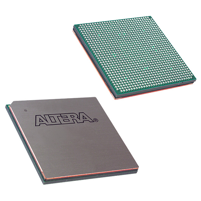
Digital Micromirror Device (DMD) is a type of micro-electromechanical system (MEMS) widely used in Digital Light Processing (DLP) projection technology. It consists of an array of microscopic mirrors that can tilt to reflect light, thereby creating an image.
How DMD works: The DMD technology utilizes hundreds of thousands to millions of microscopic mirrors that can independently tilt to reflect light, which is then projected to form a high-quality image.

DMD Technology Application Solutions Overview
Explore the diverse applications of Digital Micromirror Device (DMD) technology in various industries. Below are the key application areas and the corresponding solution options based on performance and cost requirements.
Projection Displays
Application Goal: Provide high-quality image output, suitable for home, commercial, and micro-projectors.
Solutions:
- High-Performance: High resolution and brightness for premium projectors.
- Balanced: Medium resolution and brightness for most applications.
- Low-Cost: Lower resolution and brightness for budget-friendly projectors.

Automotive HUD (Head-Up Display)
Application Goal: Enhance driving experience by projecting navigation, speed, and warnings onto the car windshield.
Solutions:
- High-Performance: High brightness and resolution for clear visibility in various lighting conditions.
- Balanced: Good visibility and brightness for general driving environments.
- Low-Cost: Basic functionality suitable for entry-level vehicle systems.

Adaptive Headlights (ADB)
Application Goal: Adjust headlight brightness and angle based on road, vehicle speed, and ambient light.
Solutions:
- High-Performance: Precise control for dynamic lighting adjustment.
- Balanced: Moderate precision for most driving conditions.
- Low-Cost: Basic functionality for standard headlights.

Industrial 3D Printing
Application Goal: Utilize DMD technology to control light sources for high-precision lithography in 3D printing.
Solutions:
- High-Performance: High resolution for precise 3D printing applications.
- Balanced: Medium resolution for most industrial applications.
- Low-Cost: Lower resolution for budget printing needs.

Laser Processing
Application Goal: High-precision laser cutting, welding, and engraving of metals and other materials.
Solutions:
- High-Performance: High power and precision for industrial laser equipment.
- Balanced: Medium power for general processing tasks.
- Low-Cost: Lower power for budget-friendly applications.

Medical Imaging
Application Goal: Provide high-resolution imaging for diagnostic purposes in medical devices.
Solutions:
- High-Performance: Ultra-high resolution for advanced medical imaging systems.
- Balanced: Medium resolution for general medical equipment.
- Low-Cost: Basic resolution for entry-level medical devices.

Optical Imaging Systems (Spectral Analysis)
Application Goal: Provide precise light source control for optical instruments like spectrometers and optical detectors.
Solutions:
- High-Performance: High precision for critical optical measurements.
- Balanced: Medium precision for general optical applications.
- Low-Cost: Basic functionality for non-critical applications.

Virtual Reality & Augmented Reality (VR/AR)
Application Goal: Use DMD technology for optical imaging and display in VR/AR devices.
Solutions:
- High-Performance: High resolution and low latency for immersive VR/AR experiences.
- Balanced: Good resolution and performance for most VR/AR applications.
- Low-Cost: Lower resolution for basic VR/AR setups.

High-Precision Laser Scanners
Application Goal: High-precision scanning, measurement, and detection applications using laser technology.
Solutions:
- High-Performance: High resolution and accuracy for precision scanning.
- Balanced: Medium resolution for general scanning tasks.
- Low-Cost: Basic resolution for affordable laser scanning solutions.

Photolithography / Microelectronics Manufacturing
Application Goal: Use DMD technology in photolithography for precise patterning in semiconductor manufacturing.
Solutions:
- High-Performance: Ultra-high precision for advanced photolithography.
- Balanced: Medium precision for standard microelectronics manufacturing.
- Low-Cost: Lower precision for entry-level microelectronics applications.

Projection Displays
3.1 Application Goal
Application Goal: Achieve high-resolution projection with energy efficiency and long lifespan, suitable for home theaters, commercial projectors, and micro-projectors.
Digital Micromirror Device technology enables high-quality, long-lasting projection with excellent image clarity for home theaters, business venues, and portable devices.

3.2 Three Solutions Comparison
Goal: Provide three configurations to clarify performance-versus-cost trade-offs.
Solution A: High-Performance
Features: High-end Digital Micromirror Device + high-efficiency power management + high-resolution support.
Use Cases: Premium home theater, large commercial projection.
Solution B: Balanced
Features: Mid-range Digital Micromirror Device + mainstream power management + medium resolution.
Use Cases: Business/classroom projectors, everyday use.
Solution C: Cost-Optimized
Features: Cost-effective Digital Micromirror Device + basic power management + lower resolution.
Use Cases: Entry-level home projectors, small meeting rooms.
3.3 Chip Combination Logic
Goal: Explain how multi-vendor chips combine into a complete projection solution.
Power Management Chip Selection
- TI TPS7A16 — low-noise LDO for sensitive rails.
- ST LD39050 — balanced noise and transient response.
- Microchip MCP1700 — ultra-low quiescent current for cost-sensitive, portable use.
Driver / Interface Selection
- TI interface/driver families for robust high-speed signaling.
- onsemi options where automotive-grade robustness is required.
- NXP industrial-oriented transceivers for harsh EMI environments.
3.4 Packaging and Signal Considerations
Goal: Clarify why certain packages and interfaces are chosen and how they align with Digital Micromirror Device requirements.
Packaging Choice
For higher power density and thermal headroom, QFN is often preferred over BGA in compact projection engines due to superior heat spreading and simpler assembly.
Signal Interfaces
MIPI and LVDS are commonly used for high-speed image data into the controller; robust differential links help with EMI. RS-485 may appear in peripheral/industrial control paths.
3.5 Trade-Off Choices
Goal: Help users select based on price, lifetime, and performance.
- Lifetime-first: Choose Solution A for long service life and image stability.
- Balanced budget/performance: Choose Solution B.
- Cost-first: Choose Solution C for entry-level deployments.
3.6 Underlying Design Principles
Projection with a Digital Micromirror Device generally follows: prioritize image fidelity (resolution/contrast), maintain thermal/EMI margins, and balance efficiency versus brightness for the intended venue size.
Automotive HUD (Head-Up Display)
Application description: Project critical driving information (navigation, speed, ADAS warnings) onto the windshield/combiner to reduce eye-off-road time and improve safety.

3.1 Application Goal
Goal: Deliver bright, high-contrast, low-latency visuals that remain readable under sunload, with a wide field of view (FOV) and generous eyebox for diverse driver positions.
Digital Micromirror Device technology enables fast light modulation and high optical efficiency, helping HUD systems achieve windshield legibility day and night.
3.2 Three Solutions Comparison
Objective: Present three configurations to clarify performance vs. cost trade-offs.
Solution A — High-Performance
- High-power multi-channel light source (LED/laser), automotive PMIC, high-speed DMD control, wide FOV/eyebox.
- Use cases: Premium passenger vehicles requiring maximum brightness margin and durability.
Solution B — Balanced
- Mid-power light engine, mainstream PMIC, standard DMD configuration, balanced FOV and BOM.
- Use cases: Volume models seeking a “good-enough” mix of readability, cost, and thermal profile.
Solution C — Cost-Optimized
- Simplified light path, reduced FOV/eyebox, basic power rails and interfaces for entry trims.
- Use cases: Entry vehicles or regional variants prioritizing BOM cost.
3.3 Chip Combination Logic
Objective: Show neutral, multi-vendor options that commonly combine into an automotive HUD system.
- Power (quiet/sensitive rails): low-noise LDOs (e.g., TI TPS7A16-Q1, ST LD39050, Microchip MCP17xx family) or automotive-grade equivalents.
- Main DC/DC: automotive buck regulators from onsemi / Renesas / NXP selected by current/efficiency/EMI targets.
- Light-source drivers: LED/laser drivers from TI / onsemi / Renesas chosen by channel count, dimming method, and thermal budget.
- Video/SerDes & control: bridge/SerDes from TI (e.g., FPD-Link families), NXP, or Microchip; controller/SoC from NXP/Renesas depending on graphics pipeline and interfaces.
- Monitoring & sensing: temperature/current/ambient-light sensing from Melexis / ST for brightness and thermal protection loops.
3.4 Packaging & Signal Considerations
- Packaging: Compact engines often prefer QFN/PowerQFN for heat spreading and assembly robustness; BGA is used where pin-count/bandwidth demands justify it, with attention to reflow and board stack-up.
- Signals: High-speed image paths commonly use MIPI/LVDS into controller & SerDes; maintain controlled impedance, differential symmetry, and EMI margins. Light-driver switching transients require tight return paths and filtering.
3.5 Trade-Off Choices
- Lifetime-first: Choose Solution A (brightness headroom, lower junction temps, robust thermal design).
- Cost-first: Choose Solution C (simplified optics/FOV, fewer channels, smaller PMIC set).
- Balanced TCO: Solution B for mainstream programs balancing readability, EMI/EMC, and BOM.
3.6 Underlying Design Principles
Prioritize safety readability under sunload, then thermal/lifetime margins, then cost. In practice, HUD success hinges on differential signal integrity (SerDes/bridges) and quiet power rails (PSRR/ripple/ground return) around the Digital Micromirror Device light engine.
Adaptive Headlights (ADB)
Application description: Adjust beam shape and brightness based on road, speed, ambient light, and oncoming traffic to deliver glare-free high beams and precise illumination.

3.1 Application Goal
Goal: Deliver high-luminance, glare-free illumination with fine-granularity beam shaping and millisecond response across day/night and adverse weather conditions.
Using a Digital Micromirror Device, the lighting ECU dynamically redistributes light to brighten relevant regions (lanes, signage, curves) while shading oncoming vehicles, improving safety and comfort.
3.2 Three Solutions Comparison
Objective: Quantify trade-offs rather than describe them.
| Item | Solution A — High-Performance | Solution B — Balanced | Solution C — Cost-Optimized |
|---|---|---|---|
| Light engine (electrical) | 80–150 W multi-channel LED/laser | 40–80 W multi-channel LED | 20–40 W LED |
| Effective road zones | ≥ 1024 | 512 | 256 |
| Update rate | ≥ 120 Hz | 60–90 Hz | ~60 Hz |
| Thermal budget (θja target) | < 1.2 °C/W module-level | ~1.6 °C/W | ~2.0 °C/W |
| EMI margin vs CISPR 25 | > 6 dBμV headroom | ~3 dBμV | 0–3 dBμV |
| Typical vehicle fit | Premium/flagship | Volume models | Entry trims/regional |
| BOM impact | High (multi-channel drivers, larger optics) | Medium | Low (simplified optics/FOV) |
Solution C — Cost-Optimized
- Simplified optical path, reduced projection area, basic power rails/interfaces.
- Use cases: Entry trims or regional variants prioritizing BOM cost over maximum resolution.
3.3 Chip Combination Logic
Objective: Show neutral, multi-vendor options commonly combined in ADB systems; selection is driven by PSRR/noise, efficiency/thermals, EMI/EMC, and automotive qualifications.
- Power (quiet/sensitive rails): low-noise LDO families such as TI TPS7Axx-Q1, ST LD39xxx, Microchip MCP17xx for controller/Digital Micromirror Device sensitive rails.
- Main DC/DC: automotive buck regulators from onsemi / Renesas / NXP sized to current and efficiency targets with spread-spectrum options for EMI.
- Light-source drivers: multi-channel LED/laser drivers from TI / onsemi / Renesas chosen by channel count, dimming strategy (PWM/analog/mixed), diagnostics, and thermal budget.
- Control & SerDes/bridges: NXP/Renesas automotive MCUs/SoCs; TI FPD-Link or alternatives from NXP/Microchip for robust differential links between ECUs and the Digital Micromirror Device controller.
- Monitoring & sensing: ambient/temperature/current sensing from Melexis / ST for closed-loop brightness and thermal protection.
3.4 Packaging & Signal Considerations
- Packaging: PowerQFN/QFN/DFN are favored for light-driver and power stages (heat spreading, assembly robustness). Use BGA/QFP where pin-count/bandwidth requires it, with careful reflow and stack-up control.
- Signals: High-speed image/control paths (MIPI/LVDS/SerDes) demand controlled impedance, differential symmetry, and EMI margin; switching transients on light drivers require tight return paths and π/LC filtering with sensible ground partitioning.
3.5 Trade-Off Choices
- Lifetime-first: Choose Solution A for brightness headroom, lower junction temperatures, and advanced diagnostics.
- Cost-first: Choose Solution C by reducing projection area/channels and simplifying PMIC/interfaces.
- Balanced TCO: Solution B offers practical readability with manageable EMI/thermals and BOM.
3.6 Underlying Design Principles
Prioritize traffic safety and glare control, then thermal/lifetime and EMC robustness, and finally cost optimization. Successful ADB implementations hinge on differential signal integrity and quiet power rails around the Digital Micromirror Device light engine, synchronized with perception ECU strategies.
Industrial 3D Printing (DLP Mask Projection)
Application description: Use a Digital Micromirror Device to spatially modulate UV/visible light and polymerize photosensitive resin layer-by-layer for high-precision lithography-style 3D printing.

3.1 Application Goal
Goal: Achieve lithography-grade XY precision and stable layer curing while maximizing build rate and uniformity across the field.
| KPI | Target / Typical Range | Notes |
|---|---|---|
| XY pixel size at resin plane | 25–75 μm (telecentric), up to 100–150 μm (cost-optimized) | Pixel = mirror pitch / |M|, where |M| is optical reduction |
| Layer thickness (Z) | 25–100 μm | Set by resin, optics DOF, and Z mechanics |
| Uniformity (across build area) | ±10% irradiance | Flat-field correction via Digital Micromirror Device and optics |
| Wavelength | 385–405 nm | 385 nm for finer features; 405 nm broader resin availability |
| Irradiance at resin | 5–20 mW/cm² | Per layer exposure 1–6 s typical (depends on resin working curve) |
| Build area | ~50×30 mm (high-res) to 192×120 mm (balanced) to 250×140 mm (cost) | Scales inversely with resolution at fixed Digital Micromirror Device size |
| System stability | XY drift < 10 μm / hr | Thermal & mechanical stability of optical engine |
| EMI/ESD | EN 55032 Class B, IEC 61000-4-x | Industrial printers for lab/office environments |
3.2 Three Solutions Comparison
Objective: Quantify differences in optics, power and performance instead of generic descriptions.
| Item | Solution A — High-Performance | Solution B — Balanced | Solution C — Cost-Optimized |
|---|---|---|---|
| Digital Micromirror Device / optics | High-res Digital Micromirror Device, telecentric reduction |M|≈2–3×; AR-coated UV glass | Standard Digital Micromirror Device, |M|≈1.5–2× | Standard Digital Micromirror Device, simple projection |M|≈1–1.5× |
| XY pixel @ resin | 25–40 μm | 50–75 μm | 100–150 μm |
| Build area (typ.) | ~80×45 mm | ~192×120 mm | ≥ 220×130 mm |
| UV source power (electrical) | 60–120 W (385 nm LED/laser) | 40–80 W (405 nm LED) | 20–40 W (405 nm LED) |
| Uniformity after FFC | ±5–8% | ±10% | ±15% |
| Throughput (example) | 30–60 mm/h @ 50 μm layers | 20–40 mm/h @ 75 μm | 15–25 mm/h @ 100 μm |
| BOM/complexity | High (telecentric optics, higher UV power, active cooling) | Medium | Low (simpler lens stack, passive cooling) |
3.3 Chip Combination Logic (neutral, multi-vendor)
- Power for sensitive rails: low-noise LDOs (noise < 10–20 μVrms, PSRR > 60 dB @ 1 kHz) for Digital Micromirror Device controller/PLL and reference rails.
- Main DC/DC: 2–10 A bucks ≥ 92% efficiency; synchronize or spread-spectrum to keep EMI below EN 55032 peaks; soft-start to avoid Digital Micromirror Device brownout.
- UV LED/laser drivers: constant-current with analog + PWM dimming, 0.5–3 A/channel, kHz-level PWM (avoid banding); include NTC feedback and open/short diagnostics.
- Imaging/IO: MIPI/LVDS links from controller/SoC to the Digital Micromirror Device controller; position/limit inputs for Z-stage; optional photodiode feedback ADC for dose control.
- Sensing/monitoring: temperature/current monitors for lamp and optics; ambient & stray-UV monitoring for safety interlock (EN 60825 considerations for laser variants).
3.4 Packaging & Signal Considerations
- Packaging: Use QFN/DFN/PowerQFN for drivers and PMICs (low θJA); reserve copper pours under hot devices; keep Digital Micromirror Device controller on a low-noise island with star-ground return.
- Differential routing: 100 Ω ±10% for LVDS/MIPI, intra-pair skew < 10 ps/cm; short stubs and matched lengths into the Digital Micromirror Device controller.
- Optical stack: Prefer telecentric projection for uniform pixel geometry; use quartz/UV-grade glass; minimize outgassing materials near the Digital Micromirror Device and resin vat.
3.5 Trade-Off Choices
Working-curve (cure depth): C_d = D_p · ln(E / E_c), where C_d is cured depth, D_p penetration depth (typically 0.08–0.20 mm at 385–405 nm), E dose (mJ/cm²), E_c critical dose (5–15 mJ/cm² resin-dependent).
Dose sizing: E = I · t (mJ/cm²), where I is irradiance at resin (mW/cm²) and t exposure time (s). Keep C_d ≈ 1.2–1.8× layer thickness for inter-layer adhesion without over-cure.
- Resolution-first: choose Solution A, smaller pixel & telecentric optics; accept smaller build area and higher UV power/cooling.
- Throughput-first: maximize irradiance & duty cycle; balance with resin exotherm and shrinkage.
- Cost-first: choose Solution C, larger pixels and simpler optics; rely on Digital Micromirror Device flat-field & software compensation.
3.6 Underlying Design Principles
- Lock XY pixel geometry first (Digital Micromirror Device + projection reduction), then size UV power to meet resin dose with margin.
- Design uniformity (optics + Digital Micromirror Device flat-field) before chasing throughput; uneven cure dominates dimensional error.
- Keep Digital Micromirror Device/PLL rails quiet; exposure banding and pixel jitter often trace to PSRR/ground-return issues rather than software.
Laser Processing (Cutting • Welding • Micromachining)
Application description: Use a Digital Micromirror Device (DMD) to dynamically shape or multiplex the beam for metal cutting, welding seam tailoring, and precision engraving/texturing.

3.1 Application Goal
Goal: Achieve stable, high-throughput processing with fine spatial control and millisecond-class updates.
3.2 Three Solutions Comparison
Objective: Quantify differences rather than describe them.
- Laser/LED: 1–3 kW fiber or 200–500 W UV/visible; multi-spot via DMD.
- Effective zones: ≥ 1024; update ≥ 120 Hz.
- Thermal/EMI margin: > 6 dBμV; active cooling for optics & DMD.
- Laser/LED: 500–1500 W fiber or 100–200 W UV.
- Effective zones: ~512; update 60–90 Hz.
- Thermal/EMI margin: ~3 dBμV; mixed cooling.
- Laser/LED: 200–500 W fiber or 50–100 W UV.
- Effective zones: ~256; update ~60 Hz.
- Simplified optics; passive cooling; minimal EMI headroom.
3.3 Chip Combination Logic (neutral, multi-vendor)
- Power (quiet rails): low-noise LDOs (noise < 10–20 μVrms, PSRR > 60 dB@1 kHz) for DMD controller/PLL rails.
- Main bucks: 2–10 A, ≥ 92% efficiency; synchronize/spread-spectrum to avoid EMI peaks during high-power switching.
- Laser/LED drivers: 1–10 A/channel, analog+PWM dimming at ≥ 2–4 kHz, with NTC feedback and open/short diagnostics.
- SerDes/bridges: LVDS/MIPI/FPD-Link class; maintain eye margin at the longest harness length in the cell.
- Monitoring: temperature/current/photodiode feedback for closed-loop irradiance and safety interlocks.
3.4 Packaging & Signal Considerations
- Packages: QFN/PowerQFN/DFN for drivers & PMIC (low θJA); BGA/QFP where bandwidth/pin-count require, with controlled reflow/stack-up.
- Differential links: 100 Ω ±10% for LVDS/MIPI; minimize intra-pair skew; keep stubs short into the DMD controller.
- Ground/returns: Keep driver loop area small; π/LC at supply entry; star-point ground to isolate noisy returns from DMD rails.
3.5 Trade-Off Choices
Optical power quick-check: Required power density ≈ q = P / A. For multi-spot, P_total = Σ P_i; DMD efficiency and optics transmission set practical limits.
- Throughput-first: more spots at lower per-spot power (parallelism) until material interaction limits.
- Precision-first: smaller spot/NA, slower feed, tighter thermal control.
- Cost-first: Solution C with reduced zones and simpler optics; accept lower parallelism.
3.6 Underlying Design Principles
- Lock beam quality (M²/NA/spot size) and DMD mapping first; then scale power and parallelism.
- Design EMI/thermal headroom early; late fixes multiply optics and shielding cost.
- Most artefacts trace back to noisy rails or return paths near the Digital Micromirror Device controller—treat them as first-order risks.
Medical Imaging (Microscopy • Endoscopy • Surgical Visualization)
Application description: A Digital Micromirror Device (DMD) spatially modulates illumination for high-resolution medical imaging — e.g., structured-illumination microscopy (SIM), confocal-like optical sectioning, hyperspectral/endoscopic projection, and surgical microscopes.

3.1 Application Goal
Goal: Deliver optical-sectioned, high-contrast images with precise dose control and low latency, suitable for clinical/biolab use.
3.2 Three Solutions Comparison
Objective: Quantify trade-offs for resolution, field size, dose and cost.
- Telecentric reduction |M|≈2–4×, high-NA objectives (≥0.75).
- Pattern rate 9–20 kHz; effective pixel 1–2 μm; uniformity ±5%.
- Multi-line lasers + precision drivers; synchronized sCMOS.
- |M|≈1.5–2×, NA 0.5–0.75.
- Pattern rate 3–9 kHz; pixel 2–4 μm; uniformity ±8–10%.
- High-power LED set (385/405/488/520/635 nm) with photodiode feedback.
- Simple projection |M|≈1–1.5×, NA 0.3–0.5.
- Pattern rate 1–3 kHz; pixel 4–8 μm; uniformity ±12–15%.
- LED-only, basic dose control; entry-level camera.
3.3 Chip Combination Logic (neutral, multi-vendor)
- Power — quiet rails: low-noise LDOs for Digital Micromirror Device controller/PLL (noise < 10–20 μVrms, PSRR > 60 dB @ 1 kHz). Families from TI (TPS7Axx), ST (LD39xxx), Microchip (MCP17xx).
- Main bucks: 2–6 A, ≥92% efficiency; soft-start and spread-spectrum (onsemi, Renesas, NXP).
- Light drivers: laser/LED constant-current 0.3–1.5 A/ch, analog+PWM dimming, APC/ACC, fault & NTC (TI, onsemi, Renesas).
- Imaging & links: MIPI/LVDS from SoC/MCU to the Digital Micromirror Device controller; camera via MIPI/USB3; robust SerDes (TI FPD-Link / NXP / Microchip) if distance demands.
- AFE & sensing: photodiode TIA → 16-bit ADC for dose; temperature/ambient monitoring (ST/Melexis) for closed-loop exposure.
3.4 Packaging & Signal Considerations
- Packages: QFN/DFN/PowerQFN for drivers/PMIC (low θJA); BGA/QFP for SoC/FPGA. Keep the Digital Micromirror Device controller on a low-noise island, star-grounded.
- Differential links: 100 Ω ±10% for LVDS/MIPI; short stubs; intra-pair skew < 10 ps/cm; guard sensitive TIA nodes from fast Digital Micromirror Device edges.
- Optics/cleanliness: Telecentric projection reduces keystone; AR/UV-grade windows; avoid outgassing near the Digital Micromirror Device and sterile path.
3.5 Trade-Off Choices
Geometry: effective sample pixel p ≈ pDMD / |M|; field size scales with array size / |M|. Match p to optical resolution (≈ 0.61·λ / NA).
Dose control: exposure E = I · t; manage photobleaching by keeping E just above the SNR threshold and using higher NA rather than brute-force intensity.
- Resolution-first: choose Solution A (higher NA, telecentric optics, lasers).
- Throughput-first: increase pattern rate and camera fps with moderate NA (Solution B).
- Cost-first: Solution C with LED-only and larger pixels; rely on Digital Micromirror Device flat-fielding.
3.6 Underlying Design Principles
- Lock optical resolution (λ, NA) and Digital Micromirror Device mapping first; size illumination power only after pixel geometry is fixed.
- Synchronize triggers (Digital Micromirror Device ↔ camera) early; most artefacts are timing or quiet-rail issues, not algorithms.
- Design for medical compliance and cleaning: low-outgassing materials, sealed optics, IEC 60601/60825 margins.
Optical Imaging & Spectral Analysis
Application description: A Digital Micromirror Device (DMD) provides programmable apertures, coded masks, and wavelength selection for spectrometers and optical test instruments that require precise, repeatable light control.

3.1 Application Goal
Goal: Deliver high-SNR spectra/images with precise wavelength selection, fast pattern updates, and minimal stray light over the required band.
3.2 Three Solutions Comparison
Objective: Quantify resolution, band, speed and cost to clarify trade-offs.
- Telecentric optics; diffraction grating + DMD coded aperture (Hadamard/compressive patterns).
- Resolution 0.1–0.3 nm (VIS); update 5–10 kHz; SNR > 800:1 @ 1 s.
- Dual detectors option (CCD+InGaAs) for 400–1700 nm with stitching.
- Standard imaging spectrometer; DMD programmable slit/scanner.
- Resolution 0.5–1.0 nm (VIS); update 1–3 kHz; SNR > 500:1.
- Band 400–1000 nm (sCMOS/CCD) or 900–1700 nm (InGaAs).
- Simplified optics; DMD as static/step-scan slit; LED source.
- Resolution 1–3 nm; update 100–500 Hz; SNR > 200:1.
- Band 450–800 nm; compact form factor for portable testers.
3.3 Chip Combination Logic (neutral, multi-vendor)
- Quiet rails: low-noise LDOs for DMD controller/PLL and detector clocks (noise < 10–20 μVrms, PSRR > 60 dB @ 1 kHz).
- Main DC/DC: 2–6 A bucks ≥92% efficiency; spread-spectrum or synchronization to limit EMI near detector/TIA bands.
- Detector AFE: low-noise TIA (e.g., input noise < 5–10 pA/√Hz), 16–24-bit ADC; TEC drivers for InGaAs with ±0.1 °C stability.
- Light drivers: LED/laser constant-current 0.1–1.0 A/ch, PWM ≥ 2–5 kHz; photodiode APC/ACC for radiometric stability < 0.2%/hr.
- Links/Timing: MIPI/LVDS/FPD-Link from SoC/MCU to DMD controller; hardware triggers to synchronize patterns and exposure.
3.4 Packaging & Signal Considerations
- Packages: QFN/DFN for PMIC/drivers (low θJA); BGA/QFP for SoC/FPGA. Keep detector AFE isolated from fast DMD edges; star-ground strategy.
- Differential links: 100 Ω ±10% for LVDS/MIPI; intra-pair skew < 10 ps/cm; short stubs into the DMD controller and camera.
- Opto-mechanics: Stray-light control with baffles/black coatings; flat-field and wavelength calibration (NIST-traceable) stored in non-volatile memory.
3.5 Trade-Off Choices
Resolution: R = λ / Δλ; for imaging spectrometers, Δλ ≈ w / (D · M), where w is effective slit width (set by DMD pixel group), D is reciprocal linear dispersion (nm/mm) at the detector, and M is magnification.
SNR model: SNR = S / √(S + D + σread²), improved by Hadamard coding (≈√N when detector-noise-limited). Keep exposure below detector well capacity; stabilize source with APC.
- Resolution-first: narrow DMD slit (few pixels), telecentric optics, slower scan → Solution A.
- Speed-first: wider slit + coded patterns, higher pattern rate → Solution B.
- Cost-first: single-band LED source, simple optics, step scanning → Solution C.
3.6 Underlying Design Principles
- Fix pixel geometry and DMD-to-detector mapping first; resolution follows from slit width and dispersion.
- Calibrate wavelength, flat-field, and dark current routinely; store temperature coefficients for both detector and source.
- Guard quiet rails and AFE layout—most artefacts in spectra come from EMI/ground return, not algorithms.
Virtual & Augmented Reality (VR/AR)
Application description: A Digital Micromirror Device (DMD) serves as a high-speed microdisplay / light modulator for near-eye VR headsets and AR waveguide projectors, enabling bright, high-contrast imaging and time-sequential color.

3.1 Application Goal
Goal: Deliver bright, low-latency near-eye visuals with comfortable FOV and angular resolution, while meeting eye-safety and thermal limits.
3.2 Three Solutions Comparison
Objective: Clarify the trade-offs among resolution/FOV, brightness and cost.
- Digital Micromirror Device microdisplay ≥ 1080p per eye, 120 Hz; pixel pitch ~5–7 μm; waveguide with pupil replication.
- Laser or high-radiance RGB LED with fast drivers; exit luminance > 3000 nits (AR) or > 150 nits (VR).
- Inside-out tracking + eye tracking; low-persistence scanout.
- 720p–1080p, 90–120 Hz; RGB LED sequential color; simple waveguide/combiner.
- Exit luminance 1200–2000 nits (AR) / 80–120 nits (VR); FOV 35–45° (AR) or ~100° (VR).
- IMU + camera fusion; optional eye-tracking for foveation.
- 0.2–0.3″ Digital Micromirror Device WVGA–720p, 60–90 Hz; compact optics.
- Exit luminance 600–1200 nits (AR) / 60–90 nits (VR); FOV 25–35° (AR) or ~90° (VR).
- LED-only light engine; basic 3-DoF IMU tracking.
3.3 Chip Combination Logic (neutral, multi-vendor)
- Power (quiet rails): low-noise LDOs for Digital Micromirror Device controller/PLL (noise < 10–20 μVrms, PSRR > 60 dB@1 kHz).
- Main DC/DC: 2–6 A bucks ≥ 92% efficiency; spread-spectrum/sync to avoid EMI in IMU/camera bands.
- LED/laser drivers: 0.3–1.5 A/ch, analog+PWM (≥ 2–5 kHz) for time-sequential color; photodiode APC for radiometric stability.
- Links & control: MIPI-DSI/LVDS from SoC to Digital Micromirror Device controller; SerDes for remote light engine; IMU/SLAM sensor hub.
- Eye/hand tracking: compact cameras + VCSEL/LED illumination with IEC 60825 guards; low-power ISP.
3.4 Packaging & Signal Considerations
- Packages: QFN/DFN/PowerQFN for drivers/PMIC; BGA/QFP for SoC/FPGA. Keep Digital Micromirror Device controller on a low-noise island; star-ground returns.
- Differential links: 100 Ω ±10% for MIPI/LVDS; intra-pair skew < 10 ps/cm; short stubs into the controller.
- Thermals: limit near-eye surface rise (< 2–3 °C); spreader/graphite sheets; derate duty for laser engines.
3.5 Trade-Off Choices
Angular pixel quick-check: θpix (arcmin) ≈ 3438·p/feff. For p=5.4 μm and feff=35 mm, θ ≈ 0.53 arcmin (retina-class).
Brightness/etendue: Asrc·Ωsrc ≈ Aexit·Ωexit/η. To raise eyebox nits, increase source radiance, efficiency η, or shrink exit etendue (trade-offs with FOV/eyebox).
- Clarity-first: Solution A (higher pixel density, 120 Hz, pupil replication).
- Comfort/battery-first: Solution B with LED engine and efficient optics.
- Cost/weight-first: Solution C with compact optics and moderate FOV.
3.6 Underlying Design Principles
- Fix pixel geometry and FOV early; latency and etendue budgets follow from these constraints.
- Guard quiet rails around the Digital Micromirror Device controller—most artefacts (color breakup, banding) trace to power/EMI, not content.
- Meet eye-safety and thermal limits before chasing peak nits; comfort wins long sessions.
High-Precision Laser Scanners (Metrology • Inspection)
Application description: A Digital Micromirror Device (DMD) spatially modulates laser/LED light to generate structured-light patterns or multi-spot scans for precise measurement, inspection, and 3D reconstruction.

3.1 Application Goal
Goal: Achieve fast, high-accuracy scans with repeatable geometry and low speckle/stray light over industrial ranges.
3.2 Three Solutions Comparison
Objective: Clarify speed/accuracy/BOM trade-offs using concrete targets.
- Telecentric projection; high-radiance laser w/ speckle mitigation; DMD ≥ 10 kHz patterns.
- Angular step ≤ 60 μrad; point placement ≤ 10–20 μm @ 1 m; depth precision 0.05–0.10 mm.
- Dual cameras (global-shutter sCMOS); factory calibration & thermal compensation.
- Standard projection; laser or high-power LED; DMD 3–10 kHz patterns.
- Angular step 80–120 μrad; placement 20–40 μm; depth 0.10–0.20 mm.
- Single camera + calibrated baseline; moderate BOM and cooling.
- Compact optics; LED source; DMD 0.5–3 kHz patterns.
- Angular step 120–200 μrad; placement 40–80 μm; depth 0.20–0.50 mm.
- Simplified calibration; passive cooling; smallest BOM.
3.3 Chip Combination Logic (neutral, multi-vendor)
- Quiet rails: low-noise LDOs for the Digital Micromirror Device controller/PLL (noise < 10–20 μVrms, PSRR > 60 dB@1 kHz).
- Main bucks: 2–6 A, ≥ 92% efficiency; spread-spectrum/sync to avoid EMI in camera/TIA bands.
- Laser/LED drivers: 0.3–2 A/ch, analog+PWM (≥ 2–5 kHz); photodiode APC for < 0.2%/h stability.
- Sensor chain: global-shutter sCMOS; low-noise TIA and 16-bit ADC for photodiode feedback.
- Links/timing: MIPI/LVDS from SoC/FPGA to Digital Micromirror Device controller; hardware triggers to lock pattern-exposure timing.
3.4 Packaging & Signal Considerations
- Packages: QFN/PowerQFN/DFN for drivers/PMIC; BGA/QFP for SoC/FPGA. Keep the Digital Micromirror Device controller on a low-noise island; star-ground.
- Differential links: 100 Ω ±10% for LVDS/MIPI; intra-pair skew < 10 ps/cm; very short stubs into controller/camera.
- Opto-mechanics: Matte black internals, baffles; rigid mounts; thermal paths for source & controller to limit drift < 10 μm/hr.
3.5 Trade-Off Choices
Angular step: θpix ≈ pDMD/fproj (radians). Object-plane sample spacing Δx ≈ θpix·R, where R is range.
Depth precision (triangulation): σz ≈ (z²/(b·f))·σx, with baseline b, focal length f (in pixels), and image-plane localization error σx.
Throughput vs SNR: SNR ∝ √tdwell; faster scans reduce dwell time and SNR—compensate with more radiant power or coded patterns.
- Accuracy-first: Solution A; telecentric optics, small θpix, higher radiance, dual-cam calibration.
- Speed-first: Raise pattern rate and use multiplexed codes (Hadamard/Gray); Solution B.
- Cost-first: Solution C; LED engine, simpler optics, accept coarser angular step.
3.6 Underlying Design Principles
- Fix pixel geometry (θpix, FOV) and baseline early—these set the accuracy ceiling.
- Lock timing (Digital Micromirror Device ↔ camera) in hardware; most artefacts are timing/quiet-rail issues, not algorithms.
- Control stray light and speckle before chasing more power; calibration holds only if optics stay clean and stable.
Photolithography / Microelectronics Manufacturing (Maskless Lithography)
Application description: A Digital Micromirror Device (DMD) projects UV patterns onto photoresist for maskless lithography, enabling rapid iteration, small-batch semiconductor/microfluidic fabrication, and precision micro-patterning.

3.1 Application Goal
Goal: Print fine, repeatable features and overlays with controlled UV dose and field uniformity while maintaining practical throughput.
3.2 Three Solutions Comparison
Objective: Make the resolution/field/throughput trade-offs explicit.
- Telecentric reduction |M|≈4–10×, high-NA (0.25–0.35) optics; quartz/UV-grade lenses.
- CD 1–3 μm; uniformity ±5%; overlay ≤ 0.5 μm; DOF ≈ λ/(2·NA²).
- High-radiance 365/385 nm source with precision drivers; active stage with linear encoders.
- |M|≈2–4×, NA 0.15–0.25; standard UV imaging optics.
- CD 3–8 μm; uniformity ±8–10%; overlay ≤ 1 μm; moderate DOF.
- 405 nm or 385 nm LED engine; servo stage with glass-scale feedback.
- Simple projection |M|≈1–2×, NA 0.10–0.18.
- CD 8–20 μm; uniformity ±12–15%; overlay 1–2 μm.
- 405 nm LED, passive cooling; stepper stage with homing + fiducials.
3.3 Chip Combination Logic (neutral, multi-vendor)
- Quiet rails (DMD/PLL/camera clocks): low-noise LDOs (noise < 10–20 μVrms, PSRR > 60 dB @ 1 kHz).
- Main DC/DC: 2–6 A bucks ≥ 92% efficiency; spread-spectrum/sync to keep EMI away from camera/encoder bands.
- UV source drivers: constant-current with analog+PWM dimming, 0.3–3 A/ch; photodiode APC/ACC; TEC control for wavelength stability.
- Motion & feedback: servo/stepper drivers, linear encoders, limit switches; trigger I/O to sync exposure and stage settle.
- Vision alignment: CMOS camera AFE + lighting drivers; image-processing SoC/FPGA for fiducial detection.
3.4 Packaging & Signal Considerations
- Packages: QFN/DFN/PowerQFN for drivers/PMIC (low θJA); BGA/QFP for SoC/FPGA. Keep the Digital Micromirror Device controller on a low-noise island with star-ground returns.
- Differential links: 100 Ω ±10% for LVDS/MIPI; intra-pair skew < 10 ps/cm; very short stubs into DMD/camera/encoders.
- UV compatibility & cleanliness: quartz windows, low-outgassing adhesives, black anodized baffles; maintain optical cleanliness to keep CD and overlay stable.
3.5 Trade-Off Choices
Pixel mapping: wafer pixel p ≈ pDMD / |M|; choose |M| so that p ≤ CD/2 for adequate sampling (two pixels across minimum line).
Resolution & DOF: CD ≈ 0.61·λ/NA, DOF ≈ λ/(2·NA²) — raising NA improves resolution but shrinks DOF and tightens focus control.
Overlay budget: σoverlay ≈ √(σenc² + σcam² + σtherm² + σstage²); manage thermal drift and calibration cadence.
- Resolution-first: Solution A (higher |M|, higher NA, tighter mechanics and dose control).
- Throughput-first: Solution B with larger field and moderate NA; optimize step-and-repeat timing.
- Cost-first: Solution C; accept coarser CD and overlay with simpler optics/stage.
3.6 Underlying Design Principles
- Fix pixel geometry (p, |M|) and optical NA early; they set CD/DOF limits.
- Calibrate dose and flat-field first; uneven irradiance dominates CD variation.
- Guard quiet rails and grounding near the Digital Micromirror Device controller; many artefacts are power/EMI issues, not software.
Cross-Application Summary (Design Rules & Fast Decisions)
Goal: Distill reusable rules for selecting and sizing a Digital Micromirror Device solution across automotive, medical, and consumer scenarios—so teams can decide in 1–2 screens.

4.1 Executive Summary — Rules that Ship
- Compliance first, optimization second: certify to the target market, then push performance inside those boundaries.
- Lock pixel/optical geometry early: resolution, FOV, etendue dictate power, thermal, and EMI budgets.
- Quiet rails + differential integrity: most artefacts (banding/jitter) trace back to PSRR/ground return or link skew.
- Uniformity beats peak: flat, stable illumination outperforms raw lumens in every scenario.
- Neutral multi-vendor mapping: choose by function & KPIs, not brand; keep drop-in options.
- Template A/B/C: align budget–lifetime–performance expectations up front.
- Optimize one extreme at a time: chasing max resolution, max brightness, and min cost simultaneously usually fails.
4.2 Quick Decision Matrix (Automotive • Medical • Consumer)
4.3 Golden Rules (Power • Signal • Optics • Mechanics)
p ≈ pDMD/|M| first; then select NA/DOF.4.4 One-Line Constraints by Industry
- Automotive: car-grade certification + environment robustness first.
- Medical: low noise + long-term stability first.
- Consumer: value-for-money first, lifetime secondary (but monitored).
4.5 Cross-Application A/B/C Mapping
4.6 Formula Quick-Cards
FAQ — Digital Micromirror Device
Short, direct answers designed to match common PAA questions while linking into our core sections about the Digital Micromirror Device and its applications.
What is a Digital Micromirror Device?
A Digital Micromirror Device is a MEMS microdisplay made of hundreds of thousands of tilting mirrors that modulate light at high speed. It forms the core of many DLP systems for projection, heads-up displays, lithography, and scientific imaging. Read more: Introduction, Projection.
What is DMD technology?
DMD technology uses an array of hinged micromirrors to reflect light toward or away from optics, creating bright, high-contrast images. It enables fast switching, precise spatial control, and wide application coverage from projection to maskless lithography. Read more: Cross-application summary.
How does a DMD chip work?
Each mirror tilts between on/off states (typically ±12–17°), time-modulating light into gray levels; color is produced by RGB light sources or sequential filters. A controller loads bitmaps and drives the mirrors at kHz rates to render images or patterns. Read more: Projection, 3D printing.
Who invented DMD?
The Digital Micromirror Device was invented at Texas Instruments, with key patents led by Larry J. Hornbeck in the late 1980s. TI commercialized it under the DLP brand for projection and many light-control applications. Read more: Introduction.
What is the function of the DMD chip?
A Digital Micromirror Device spatially modulates light with high speed and contrast. It converts digital images into optical patterns for displays (projectors, HUD) and for industrial/medical uses (structured light, lithography, spectroscopy). Read more: HUD, Photolithography.
What type of device uses DLP?
DLP systems built around a Digital Micromirror Device appear in projectors, automotive HUD and adaptive headlights, 3D printers, maskless lithography tools, spectrometers, and near-eye VR/AR engines. Read more: Projection, ADB, Spectral analysis.
Which is better, DLP or laser projector?
They are not mutually exclusive: DLP is the imaging architecture (using a Digital Micromirror Device), while “laser projector” refers to the light source. Many high-end projectors are laser-illuminated DLP units, combining stable brightness with fast modulation. Read more: Projection.
How does a microchip actually work?
If you mean integrated circuits, billions of transistors switch to process and store information. If you mean RFID “microchips” (pets), a passive resonant tag returns an ID when powered by a reader’s field. For light control, a Digital Micromirror Device tilts mirrors to modulate light. Read more: Introduction.
Which is better, an LCD or DLP projector?
LCD often offers higher color light output at a given price; DLP with a Digital Micromirror Device tends to deliver higher native contrast, sharpness, and motion stability. Choice depends on room brightness, screen size, and budget. Read more: Projection.
What is the difference between DMD chip and DLP chip?
“DMD” is the actual micro-mirror device. “DLP” is Texas Instruments’ system/brand encompassing the Digital Micromirror Device plus its controller and optical approach. People sometimes say “DLP chip” but they mean the DMD at the heart of a DLP system. Read more: Introduction.
How does a DLP projector work?
A lamp or laser/LED source is conditioned by optics and directed onto a Digital Micromirror Device. The mirrors tilt to reflect light through a lens onto the screen; color comes from RGB sources or time-sequential color. The controller streams images to the mirrors. Read more: Projection.
What does the DMD chip stand for?
DMD stands for Digital Micromirror Device, a MEMS microdisplay comprising an array of tilting mirrors used to modulate light in DLP systems. Read more: Introduction.
Can your phone detect a microchip?
If you mean pet RFID microchips, most phones cannot read them: phones use NFC at 13.56 MHz, while pet chips commonly use 125/134.2 kHz. A dedicated scanner is required. For Digital Micromirror Device systems, phones are unrelated. Read more: Introduction.
What is the most advanced microchip?
“Most advanced” changes constantly and depends on category (logic, memory, sensors). For light modulation, a Digital Micromirror Device is a specialized MEMS microdisplay optimized for speed, contrast, and optical efficiency rather than logic density. Read more: Cross-application summary.
How long does a microchip work?
Passive RFID “microchips” can last decades since they have no battery. A Digital Micromirror Device system’s lifetime depends on optics and thermal design (often tens of thousands of hours for display engines). Read more: Projection, HUD.
Can microchips be tracked by GPS?
No—passive RFID microchips have no power source, transmitter, or GPS. Tracking requires a battery-powered device. This is unrelated to Digital Micromirror Device technology, which modulates light, not radio. Read more: Introduction.
How do you trace a microchip?
For pet RFID, scan the chip to obtain its ID, then look up the registry to contact the listed owner. This process is separate from Digital Micromirror Device systems. Read more: Introduction.
How to change microchip ownership?
Contact the RFID registry listed for the chip ID and submit ownership documentation; some regions require veterinary or shelter confirmation. This is unrelated to Digital Micromirror Device optics. Read more: Introduction.
Can a microchip be removed?
For implanted RFID, removal must be done by qualified professionals and may be regulated. This should not be confused with a Digital Micromirror Device, which is an optical component inside electronic products. Read more: Introduction.
Can a microchip show location?
Passive RFID microchips do not provide live location; they only reveal an ID when scanned by a reader. Live tracking needs GPS and a battery. This is unrelated to Digital Micromirror Device light modulators. Read more: Cross-application summary.
Can you scan a microchip?
Yes—pet RFID microchips are scanned with dedicated LF/ISO 11784/11785 readers, not with typical phones. Scanning has no connection to Digital Micromirror Device products, which control light rather than radio IDs. Read more: Introduction.
Submit Your BOM for Lead-Time Comparison & Substitution Mapping
Have a BOM or considering alternates? Upload or paste your list — we’ll compare lead times across vendors and recommend neutral, pin-compatible options for your Digital Micromirror Device–based design.
- Vendor-neutral recommendations
- Cross-vendor availability & lead-time check
- Pin/package/rail compatibility review
- Preliminary response within 48 hours*
*Adjust this SLA to your actual operations.


.png?x-oss-process=image/format,webp/resize,h_32)


